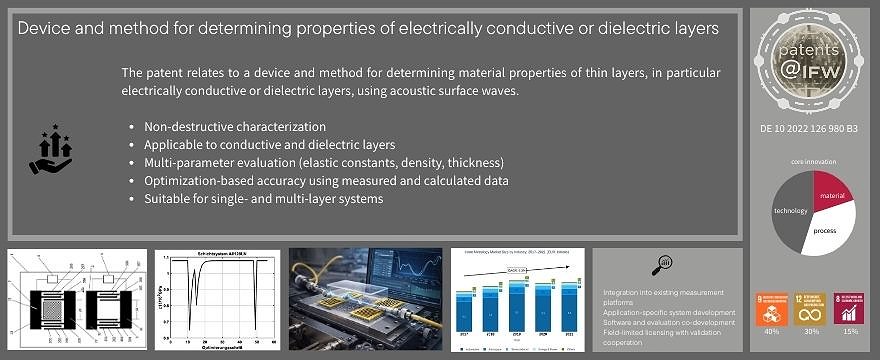
The Challenge
Determining elastic and structural properties of thin conductive or dielectric layers is often:
destructive,
limited to single parameters, or
dependent on complex sample preparation.
This restricts process control and material qualification.
The Patented Solution
A non-destructive measurement system using:
interdigital transducers generating acoustic surface waves, and
an optimization-based evaluation of frequency-dependent reflection factors.
The method enables simultaneous determination of multiple material parameters from a single measurement setup.
Key Technical Advantages
Non-destructive characterization
Applicable to conductive and dielectric layers
Multi-parameter evaluation (elastic constants, density, thickness)
Optimization-based accuracy using measured and calculated data
Suitable for single- and multi-layer systems
Application Scope
Thin-film characterization
Electronic and microsystem materials
Coating analysis and quality control
Research and industrial measurement environments
Value for License Partners
Enhanced material characterization capabilities
Integration into existing measurement and testing systems
Improved process monitoring and quality assurance
Differentiation through patented measurement methodology
Licensing Models
Device licensing
Method licensing
Application-specific licensing
Target License Partners
Manufacturers of measurement and testing equipment
Companies developing instruments for material, thin-film, or coating analysis.Suppliers of acoustic or sensor-based characterization systems
Organizations specializing in surface acoustic wave technologies.Industrial electronics and microsystems companies
Firms requiring precise, non-destructive evaluation of thin-layer materials.Research infrastructure and laboratory equipment providers
Suppliers of advanced characterization tools for R&D environments.
Options for Joint Development
Integration into existing measurement platforms
Joint development to embed the patented method into established test systems.Application-specific system development
Adaptation of the device and method to defined layer systems or materials.Software and evaluation co-development
Extension of optimization algorithms for specific industrial use cases.Field-limited licensing with validation cooperation
Licensing combined with joint experimental validation on application-relevant samples.